
GaN vs. Silicon MOSFETs in Embedded Humanoid Joint Inverters: A 2026 Engineering and Procurement Guide
Compare GaN vs silicon MOSFETs for humanoid joint inverters. Review losses, thermal limits, DC-link sizing and supplier evidence before sending a joint RFQ.
Short answer: For embedded humanoid joint inverters, GaN vs. silicon MOSFETs is a loss, packaging and validation trade-off. GaN can make higher-frequency PWM practical, especially with low-inductance motors, but silicon remains a credible embedded-drive option. Choose GaN when a measured reduction in losses or board volume justifies its cost and validation work. Neither technology guarantees a capacitor reduction, bearing lifetime, continuous torque rating or system cost saving.
Reviewed: 01 November 2026. Scope: Global OEM sourcing and electromechanical integration of electric humanoid robot joints, focusing on 48 V nominal DC buses, FOC and conduction-cooled actuator housings. Intended readers are motion-control engineers and procurement teams comparing EVT/DVT samples and volume offers. Higher-voltage drives need a separate insulation and switching review.
Method and boundaries: This is an editorial engineering synthesis of the manufacturer documents linked below, with explicit screening calculations and an RFQ decision framework. We did not bench-test these drives or obtain supplier price quotes. Calculated examples are assumptions, not measured product performance. A design-board rating is not a complete actuator rating; live pricing, lead times and safety compliance require supplier evidence.
Start with the Engineering and Sourcing RFQ Checklist, or send your joint requirements for an engineering review, including bus limits, torque-speed duty cycle and mounting conditions.
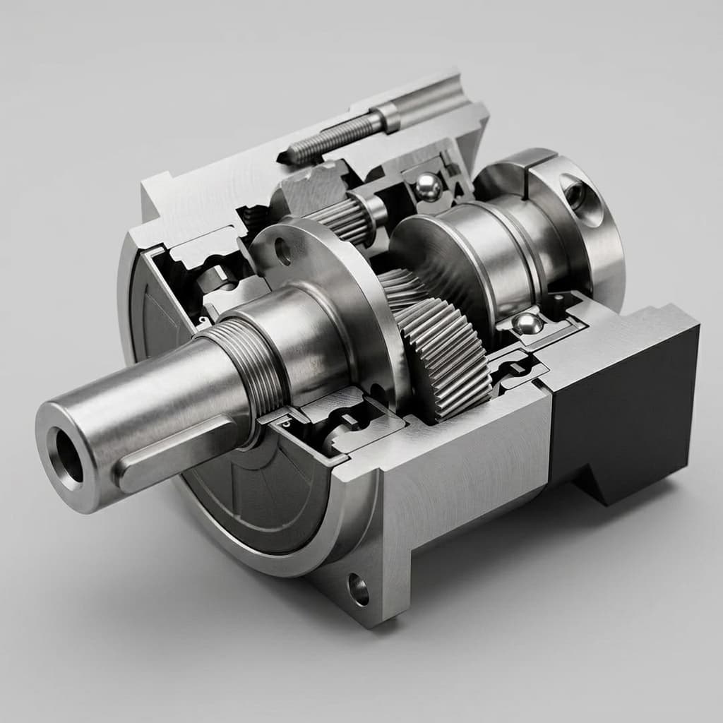
Figure 1: Illustrative mechanical cutaway. The image shows gears, bearings and a housing; it does not establish an embedded inverter, semiconductor technology, encoder configuration or tested product specification.
1. Executive Summary: The Decentralization Decision
An embedded inverter places motor control near the joint, shortening three-phase leads and changing the DC-power and communication harness. A centralized inverter may offer easier cooling and service access. The correct architecture depends on the robot's cable routing, protection, maintenance and thermal design.
Decentralization is separate from semiconductor selection: both silicon and GaN can be embedded. Harness savings from moving a drive into a joint must not be counted as an exclusive benefit of GaN.
Centralized: Battery -> inverter bay -> three-phase cables -> joint motors
Embedded:   Battery -> protected DC distribution -> local joint inverters
                                                   + communication links
Either architecture can use silicon or GaN; compare like-for-like designs.
The physical challenge is shared heat and limited board space. Assess motor winding temperature, power-stage loss, encoder limits and the housing-to-limb thermal path together. IP protection, enclosure size and sensor limits are product-specific, rather than universal requirements for every joint.
A concrete integration example is TI's TIDA-010979: a 48 V, 1 kW robot-joint reference design using three DRV7167 GaN half-bridge stages on a 70 mm PCB with a 15 mm through-hole. It demonstrates feasibility under TI's design conditions, not an industry-wide architecture standard or a sealed-joint continuous rating.
2. Electromechanical Comparison: GaN vs. Silicon MOSFETs
Compare actual device data and a common operating point rather than material-level headline numbers. Infineon's GaN portfolio overview describes potential switching-loss and power-density benefits; the magnitude requires a circuit-level comparison.
Figure 2: Conceptual selection diagram, not measured benchmark data. Both technologies require the same motor, bus and cooling boundary conditions for a fair comparison.
| Parameter / Specification | Silicon MOSFET | Enhancement-mode GaN HEMT | Evidence to request for the joint |
|---|---|---|---|
| Reverse recovery | Intrinsic body diode can add recovery loss | No PN body diode; body-diode Qrr is absent | Commutation waveforms and device data |
| Conduction loss | Set by hot on-resistance and RMS current | Same I²R dependence | Hot RDS(on), phase current and device count |
| Switching energy | Depends on device, driver and layout | Can be lower at the same operating point | Eon/Eoff or measured inverter loss map |
| Gate drive | Follow selected device voltage limits | Gate voltage and timing are device-specific | Gate waveform, driver limits and protection |
| PWM frequency | No universal silicon frequency ceiling | Higher frequency can become practical | Ripple, efficiency and control timing at chosen PWM |
| Slew rate | Tunable; can create common-mode stress | Tunable; fast edges need careful integration | Terminal dV/dt, ringing and encoder error logs |
| Dead time | Depends on delay spread and commutation | Shorter timing may be possible | Worst-case timing across current and temperature |
| DC-link storage | Ceramic, film or electrolytic can be used | Same choices; higher PWM may reduce ripple storage | Effective capacitance, ESR, ripple rating and regeneration |
| Thermal path | Cooling needed in an embedded enclosure | Cooling still needed despite lower switching energy | Thermal soak with the actual motor and mount |
| Procurement | Compare qualified, available parts | Compare qualified, available parts and support | Dated BOM, quotes, qualification and change control |
3. Mathematical Foundations: Conduction, Switching, and Thermal Scaling
A useful first estimate separates semiconductor losses from motor and control-board losses:
P_inverter = P_conduction + P_switching + P_gate + P_reverse-conduction
             + sensing, control and other board losses
P_conduction ≈ 3 × I_phase,rms² × RDS(on, hot)
P_switching ≈ f_sw × sum(Eon + Eoff for all six switches per PWM cycle)
The conduction expression assumes a balanced three-phase bridge, equal high-side/low-side resistance and synchronous conduction. It omits dead-time intervals and parallel-device imbalance. Use the actual modulation and temperature-dependent device data for final analysis. Switching energy depends on voltage, current, gate drive and layout; avoid adding separate recovery or output-capacitance loss terms if already included in Eon/Eoff.
3.1 Reproducible Screening Example: 20 A RMS Phase Current
Assumptions, not measured parts: both bridges have 4.0 mΩ hot on-resistance per switch position. Assume the sum of switching energy across all six switches is 120 µJ per PWM cycle for silicon and 30 µJ for GaN, at the selected operating point. These are illustrative inputs to replace with supplier data, not technology benchmarks.
| Assumed case | Conduction loss | Switching loss | Subtotal, excluding other losses |
|---|---|---|---|
| Silicon at 20 kHz | 3 × 20² × 0.004 = 4.80 W | 120 µJ × 20 kHz = 2.40 W | 7.20 W |
| Silicon at 80 kHz | 4.80 W | 120 µJ × 80 kHz = 9.60 W | 14.40 W |
| GaN at 80 kHz | 4.80 W | 30 µJ × 80 kHz = 2.40 W | 7.20 W |
Under these assumptions, GaN supports four times the PWM frequency with the same semiconductor-loss subtotal as silicon at 20 kHz. That is an example of the trade-off, not proof of higher robot efficiency. At the same 80 kHz, the assumed GaN subtotal is lower, but neither subtotal predicts thermal shutdown without the complete thermal path and other losses.
3.2 Turn a Loss Difference into a Thermal Question
For a fixed path, a preliminary temperature-rise estimate is temperature rise = dissipated power × thermal resistance. If an isolated board dissipates 7.2 W through an assumed 3 K/W path, its rise is 21.6 K. A motor-heated housing, shared heat paths and transient duty cycle invalidate treating this as a complete junction-temperature model.
4. DC-Link Capacitor Sizing: Ripple Is Only One Requirement
A local DC link supplies switching pulses and limits voltage ripple. A simple switched-current screening model is:
C_ripple ≈ I × D × (1 − D) / (allowed ripple × PWM frequency)
Assume I = 20 A, D = 0.5 and allowed ripple = 1 V:
At 20 kHz: C_ripple ≈ 250 µF
At 80 kHz: C_ripple ≈ 62.5 µF
This model illustrates inverse-frequency scaling for an assumed current pulse. It is not a complete three-phase capacitor design: modulation, supply impedance, ESR/ESL, ripple-current heating and DC-bias derating also matter. A fourfold frequency increase reduces this calculated ripple term by 75%; it does not guarantee 75% less installed capacitance or package volume.
Regeneration Can Dominate the Bulk-Storage Requirement
If the supply cannot absorb braking energy, use a separate energy balance:
C_energy = 2 × returned energy / (V_max² − V_initial²)
Example assumptions: 1 J returned, bus rises from 48 V to 60 V
C_energy = 2 / (60² − 48²) = 0.001543 F ≈ 1,543 µF
The 60 V endpoint is an arithmetic assumption, not an approved bus limit. Real designs need component derating and overshoot margin. A receptive supply, shared bus, braking resistor or other protection can change the required storage. Reconcile those conditions before replacing bulk capacitors with ceramics.
RFQ check: request the capacitor part numbers, effective capacitance at operating DC bias and temperature, ripple-current ratings and braking strategy. Nominal MLCC capacitance alone is insufficient; the actual derating curve is part-specific.
5. Torque Ripple, Dead Time, and Control Bandwidth
Dead time prevents simultaneous conduction in a half-bridge. Its voltage error scales approximately with bus voltage × dead time / PWM period, with polarity and magnitude depending on current and modulation. Shorter validated dead time can reduce this error; it does not remove cogging, gear ripple, current-sensor offset or all torque harmonics.
Do not assign a universal dead time or reject a supplier using a technology-wide nanosecond threshold. Require measured timing margin across temperature, current direction, driver propagation delay and fault handling.
Higher PWM can reduce current ripple in a low-inductance motor, but PWM carrier frequency, current-loop update rate and measured closed-loop bandwidth are different specifications. Ask for ADC/filter latency, control-loop timing, phase-current spectra and torque measurements at the intended speed/load. Higher carrier frequency alone proves neither battery-runtime improvement nor acoustic silence.
6. Engineering Risks and Failure Modes: Measure the Switching Edge
6.1 Common-Mode Current and Bearings
Fast phase-voltage edges can capacitively couple into the shaft, housing and sensors. A first-order relation is i = C × dV/dt; bearing discharge also depends on shaft voltage, grounding, bearing construction and lubricant film. Silicon drives can also create this stress. Semiconductor type alone does not establish bearing damage or a service-life prediction.
GaN does not inherently require 50–100 V/ns edges: EPC's EPC9176 board specifies motor-drive dV/dt below 10 V/ns. This is a useful counterexample, not a universal safe threshold. Require terminal waveforms and shaft-voltage/current measurements for the actual motor. Select edge-rate tuning, bonding, filters or bearing/shaft measures from the observed current path; ceramic bearings do not prove every discharge path has been removed.
6.2 Winding Insulation
Assess actual motor-terminal peak voltage, rise time, lead length and repetitive-pulse endurance. A 48 V embedded drive with short leads should not inherit high-voltage, long-cable industrial motor acceptance limits without analysis. Magnet-wire thermal class or enamel build alone does not qualify the complete winding insulation system. Ask the supplier which insulation-system test method and edition apply; this guide does not prescribe a universal PDIV or dielectric test voltage.
6.3 Gate Loop, Layout and Protection
Parasitic inductance can create voltage transients: an assumed 1 nH loop at 5 A/ns gives V = L × di/dt = 5 V. This is a screening illustration, not a measured gate transient. Compare actual gate-source waveforms with the selected device's limits and verify current return paths, decoupling and overcurrent response. Integrated stages can shorten critical loops, but neither integrated nor discrete construction establishes reliability by itself.
7. Whole-Body Joint Allocation: Where to Evaluate GaN vs. Silicon
Use each joint's measured duty cycle rather than a universal power/torque map. The table is an RFQ allocation framework, not published robot specifications or a mandatory semiconductor assignment.
| Joint Location / Axis | Key selection constraint | When to evaluate GaN | When silicon remains credible |
|---|---|---|---|
| Hip yaw / roll | Pelvis packaging and RMS current | Board volume or switching loss limits the design | An embedded silicon design meets the envelope |
| Hip pitch | Dynamic current and thermal cycling | Higher PWM improves measured ripple/loss balance | Conduction dominates and cooling margin is adequate |
| Knee | Holding torque and repeated peaks | Reduced switching loss materially helps the thermal budget | Hot on-resistance and current capability dominate |
| Ankle pitch / roll | Distal mass and regeneration | Verified board/capacitor savings reduce carried mass | Bus-energy storage dominates the package |
| Waist yaw / pitch | Cooling and service access | Tight board space warrants the integration work | Available mounting area supports the loss budget |
| Shoulder pitch / roll | Compact housing and sensor noise | A compact stage passes encoder/EMI checks | Existing silicon hardware is already qualified |
| Elbow | Forearm envelope and cable routing | Verified local integration improves packaging | Silicon can be embedded within the same limits |
| Wrist | Low-inductance motor and small board | Higher PWM demonstrably reduces ripple | A small silicon driver meets torque smoothness |
| Hand fingers | Multi-axis integration and low current | Integrated GaN offers a measured density benefit | Driver overhead and unit cost dominate |
| Neck | Acoustic behavior and holding duty | Measurements identify a relevant advantage | Existing silicon meets thermal/acoustic targets |
8. Supply Chain, BOM Cost, and Total Cost of Ownership
Compare embedded silicon versus embedded GaN first. Then separately compare embedded versus centralized architectures. Otherwise the cost model credits GaN for harness changes that silicon could also support.
8.1 Illustrative BOM at an Assumed 1,000-Axis Order
Planning assumptions in USD, not supplier quotes or observed 2026 market prices. Each row is an assumed cost bucket without a catalog-part claim. Prevent overlap between integrated power-stage pricing and gate-driver support when replacing these assumptions with a real BOM.
| BOM cost bucket | Assumed silicon cost / axis | Assumed GaN cost / axis | Assumed delta |
|---|---|---|---|
| Power semiconductor set | $6.50 | $16.80 | +$10.30 |
| Additional gate-drive support | $3.20 | $5.40 | +$2.20 |
| DC-link capacitors | $4.80 | $2.10 | −$2.70 |
| PCB fabrication | $2.40 | $4.20 | +$1.80 |
| Current and temperature sensing | $2.10 | $3.50 | +$1.40 |
| EMI filtering and snubbers | $1.20 | $3.10 | +$1.90 |
| Illustrative subtotal | $20.20 | $35.10 | +$14.90 |
For 32 axes, this assumed premium is 32 × $14.90 = $476.80. If the architecture change separately saves an assumed $725 in harness, connectors, enclosure and assembly, the arithmetic is $476.80 − $725 = −$248.20. These are hypothetical break-even inputs, not a promised robot saving or a GaN-specific benefit. Add NRE, qualification, yield, test, service and supply-risk costs before making a purchasing decision; do not book an unmeasured reliability saving.
8.2 Procurement Evidence That Changes the Decision
Request dated quotes at the actual annual volume, MOQ, sample/production lead time, allocation status, authorized sourcing path, lifecycle notices and change-control terms. The linked reference designs do not establish a universal price premium, current stock or delivery commitment.
For a comparable offer, send the same RFQ package for both silicon and GaN joint options, including the required operating envelope and the acceptance data below.
9. Thermal Management in Sealed Actuator Enclosures
The stator, inverter and encoder interact through the housing and mounting interfaces. Validate them as a coupled assembly rather than adding an inverter-board temperature rise to an assumed room-temperature shell.
Motor copper + iron losses ----                               -> housing + interfaces -> limb / ambient
Inverter + control losses ----/
Encoder temperature depends on location and both heat sources.
9.1 Thermal Interface Material
Choose pads, potting or mechanical interfaces from the measured heat path, tolerance stack, contact pressure and rework needs. Conductivity alone does not define interface thermal resistance. For optical sensors, review material outgassing and contamination compatibility with the encoder manufacturer; do not impose a blanket material ban without application evidence.
9.2 Encoder Thermal Margin
Record the exact encoder, switch, driver, winding and magnet ratings, including operating limits and derating. Evaluate sensor temperature and tracking errors at the worst permitted ambient and mount condition. A thermal barrier may help one path while trapping heat in another, so require measured evidence rather than a universal temperature separation or a mandated shield material.
10. Engineering and Sourcing RFQ Checklist
Use these ten questions to make offers comparable. Unknown values remain open qualification items rather than automatic passes.
- 1. Power stage: exact switch/driver BOM, voltage ratings, current definitions, layout revision and protection behavior.
- 2. PWM and control timing: carrier frequency, update rate, dead time, measured timing margin and current-loop bandwidth.
- 3. Switching waveforms: terminal dV/dt, peak voltage and ringing at minimum/maximum bus and specified current/temperature.
- 4. Bearing and grounding: shaft voltage/current evidence and justification for any bonding, filter or bearing mitigation.
- 5. Winding insulation: actual repetitive voltage stress, insulation-system qualification method and applicable test edition.
- 6. DC link and regeneration: effective biased capacitance, ripple rating, supply receptivity and worst-case braking-energy path.
- 7. Thermal path: loss map, interface construction, mounting conditions, ambient and calibrated temperature-estimation method.
- 8. Encoder margin: exact sensor rating, thermal soak and tracking/error logs with motor and inverter operating together.
- 9. Communication and safety: specified fieldbus cycle/jitter, error logs and the safety evidence required by the system risk assessment; an STO input alone does not establish SIL or PL.
- 10. Production and commercial acceptance: lot/serial traceability, agreed end-of-line tests, qualification evidence, dated price/lead-time quote and change-control terms.
11. Dyno Bench Acceptance Protocol
Proposed verification process, not a record of tests performed. Agree numerical acceptance limits before testing, based on the selected components, motor, use case and system risk assessment. Neither this guide nor a reference-board test establishes product certification.
Phase 1: Switching Waveform and Bus Audit
Use probes and an oscilloscope appropriate for the edge bandwidth, common-mode voltage and isolation requirement. Record probe loading, measurement location and test conditions. Sweep bus voltage, motoring/regenerating current and temperature. Compare peak voltage, ringing and gate waveforms against component limits with the agreed design margin. A single dV/dt number does not qualify bearings or insulation.
Phase 2: Current and Torque Ripple
Measure phase current and output torque at low speed, reversals, holding and operating load points. Record current-sensor bandwidth, torque-transducer calibration, sampling/FFT window, gear contribution and controller settings. Compare RMS current, torque ripple and measured loop response with the application specification. Use a DC-capable phase-current sensor for RMS/low-frequency measurements; a Rogowski coil alone cannot measure DC stall current.
Phase 3: Thermal Soak
Run the actual motor, encoder, enclosure and mounting interface at the maximum permitted ambient and specified continuous duty, including holding if required. Continue to a predefined equilibrium criterion rather than assuming a fixed 60-minute run is enough. Log winding, case, sensor and housing temperatures. A package thermocouple measures case temperature; estimate junction temperature with a calibrated method and suitable thermal model. Check each part's operating limit and the application's contact-surface safety requirements, rather than asserting a universal housing temperature proves compliance.
Phase 4: Common-Mode and System Integration
Measure shaft voltage and high-frequency current paths with documented probing. A temporary grounding strap changes the path under test, so interpret it accordingly. Exercise encoder, fieldbus, protection and braking behavior with the real harness and enclosure. Short tests can identify a problem; they cannot establish bearing life or field reliability. Reject or hold a sample when an agreed limit is exceeded or required evidence is absent.
12. Frequently Asked Questions (FAQ)
What is the primary physical advantage of GaN over silicon MOSFETs in a joint inverter?
Enhancement-mode GaN HEMTs have no PN body diode and therefore no body-diode reverse-recovery charge. Lower switching energy can make higher PWM frequencies practical, but conduction, output-capacitance and reverse-conduction losses remain. Compare specific devices at the same bus voltage, current and temperature.
Does GaN eliminate the thermal limit inside a sealed humanoid actuator?
No. The inverter and motor still share a housing thermal path. Continuous torque depends on winding, semiconductor, encoder and housing temperatures under the specified ambient, mounting and duty cycle. A reference-board power rating does not establish sealed-joint continuous torque.
Does a GaN inverter always switch above 50 V/ns?
No. Slew rate depends on the device, driver, layout and tuning. EPC specifies less than 10 V/ns for its EPC9176 motor-drive board. Require measurements at the motor terminals rather than assuming a GaN label establishes bearing damage or an insulation requirement.
How much more does a GaN power stage cost per joint?
There is no universal premium. Obtain dated, itemized quotes at the same volume and qualification level. Compare embedded silicon against embedded GaN separately from centralized versus embedded architectures, and include PCB, filtering, validation, supply risk and non-recurring engineering costs.
Can higher PWM frequency remove all DC-link bulk capacitance?
No. Higher PWM frequency can reduce the capacitance needed for switching ripple. Regenerative energy, supply impedance, load transients, capacitor ripple-current limits and effective capacitance under DC bias can still require bulk storage or a separate energy-absorption path.
What evidence should an OEM request before approving a GaN joint supplier?
Request the exact power-stage BOM, bus and phase-current limits, measured loss map, switching waveforms, effective DC-link capacitance, regenerative-energy strategy, thermal soak data, encoder and fieldbus error logs, and dated commercial terms. Agree acceptance limits for the actual motor and safety requirements before testing.
13. Sources & References
Manufacturer sources were checked on 01 November 2026. Their specifications apply to their own parts and reference-design conditions; none provides this guide's hypothetical costs or a market-wide adoption, pricing or lifetime forecast.
- Texas Instruments — TIDA-010979: 48 V, 1 kW robot-joint motor-control reference design. Supports the named GaN stages and 70 mm PCB / 15 mm through-hole integration example. TI identifies the board as a testing/validation reference, not a saleable joint module.
- Texas Instruments — TIDUFF7A design guide, revised March 2026. Provides the design-specific documentation structure, including power-stage, thermal-measurement, sensing and communication test sections. Use its stated setup before transferring a result to another enclosure.
- Efficient Power Conversion — EPC9176 three-phase motor-drive inverter reference design. Supports the EPC23102 stage example and motor-drive slew-rate tuning below 10 V/ns. This does not define a universal bearing-safe threshold.
- Infineon — GaN transistors (GaN HEMTs) portfolio overview. Redirects to its current transistor portfolio and explains general switching-loss, frequency and gate-driver considerations; it is not a humanoid-joint performance test.
14. Conclusion & Next Steps
Choose GaN when a fair, measured comparison shows that switching loss, current ripple or board volume constrains your joint. Retain silicon when it meets the same torque, thermal, EMI and cost requirements with a better qualification or supply position. Keep architecture savings separate, and validate regeneration and continuous thermal duty before approving either technology.
Ready to Validate Embedded Joint Actuators for Your Humanoid Program?
- Explore the humanoid joint actuator product portfolio to identify a module family for your mechanical envelope. Confirm the proposed inverter technology and ratings in the supplier's specific offer.
- Request a joint engineering and sourcing review with bus range, continuous/peak torque-speed duty, cooling mount, encoder/fieldbus requirements, quantity and destination. Ask for available drawings and validation data for that configuration before sample approval.
Author

Categories
More Posts
Rotary vs. Linear Actuators for Humanoid Robot Limbs: A 2026 Engineering and Sourcing Guide
Compare rotary vs linear actuators for humanoid robot limbs: torque mapping, roller screw trade-offs, thermal limits and sourcing. Use the 2026 RFQ checklist.
48V vs. 400V Humanoid Joint Architectures: A 2026 Procurement and Supply Chain Guide
Use this 2026 guide to compare 48V and 400V humanoid joint architectures by safety, wiring weight, TCO, supplier risk, and RFQ readiness.
Harmonic vs. Cycloidal Drives in Humanoid Joints: Navigating Fatigue Failure
Compare harmonic and cycloidal drives for humanoid robot joints, fatigue risks, shock loads, and supplier checks before selecting durable actuator modules.